Update 2015/03/08:
Added DE1 board files and a small bug fix. Fixed the repo link below to point to the right revision.
During my efforts to learn more about fpga’s I found a nice tutorial about VGA in VHDL on the DE1 board on youtube.
I was surprised how easy it is to do it when you got it explained 🙂
In short, you draw the pixel line by line on the screen and every line contains an active video phase in which the rgb pixels are sent and a blanking region which is divided into the front porch, sync pulse and back porch (see image below).
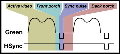
vga line
In the youtube tutorial its told that it starts with the blanking region followed by the active video phase. Probably it doesn’t matter but I did it in the same way (please comment if you know whats right and if it makes any difference).
It turned out that by starting with the visible area first the bending which was visible on the horizontal line is gone. I’ve updated the code accordingly.
The pixel clock and the pixel count of front porch, sync pulse, back porch and the active video phase is defined and can be seen here:
http://www-mtl.mit.edu/Courses/6.111/labkit/vga.shtml
http://tinyvga.com/vga-timing
I chose the resolution 640×480 with a pixel clock of 25.175 MHz. Let’s have a look at the code:
|
1 2 3 4 5 6 7 8 9 10 11 12 13 14 15 16 17 18 19 20 21 22 23 24 25 26 27 28 29 30 |
library ieee; use ieee.std_logic_1164.all; use ieee.numeric_std.all; -- http://tinyvga.com/vga-timing/640x480@60Hz ENTITY VGASYNC IS PORT( CLK: IN STD_LOGIC; -- pixel clock 25.175 MHz HSYNC,VSYNC: OUT STD_LOGIC; R,G,B : OUT STD_LOGIC_VECTOR(5 downto 0) ); END VGASYNC; ARCHITECTURE MAIN of VGASYNC IS -- Horizontal timing (line) constant hva : integer := 640; -- Visible area constant hfp : integer := 16; -- Front porch constant hsp : integer := 96; -- Sync pulse constant hbp : integer := 48; -- Back porch -- Vertical timing (frame) constant vva : integer := 480; -- Visible area constant vfp : integer := 10; -- Front porch constant vsp : integer := 2; -- Sync pulse constant vbp : integer := 32; -- Back porch signal HPOS: integer range 0 to 800:=0; signal VPOS: integer range 0 to 525:=0; |
Our vga entity will get the pixel clock as input and outputs the horizontal and vertical sync pulse together with the rgb values (6 Bit for the MiST).
Below architecture are some constants which match the given values of our resolution. HPOS and VPOS are the horizontal and vertical counters which end positions are the sums of the above values.
|
1 2 3 4 5 6 7 8 9 10 11 12 13 14 |
process(CLK) begin if rising_edge(CLK) then if HPOS < (hva+hfp+hsp+hbp) then HPOS <= HPOS + 1; else HPOS <= 0; if VPOS < (vva+vfp+vsp+vbp) then VPOS <= VPOS + 1; else VPOS <= 0; end if; end if; |
With the pixel clock we change our counters. As long as HPOS is below 800 we increase it by one. If its higher we’re in the next line and set HPOS back to zero (begin of the next line). Then we check if VPOS is below 524 and if yes increase it by one and if not set it to zero (begin of the next frame).
|
1 2 3 4 5 6 7 8 9 10 11 |
if HPOS > (hva+hfp) and HPOS < (hva+hfp+hsp) then HSYNC <= '0'; else HSYNC <= '1'; end if; if VPOS > (vva+vfp) and VPOS < (vva+vfp+vsp) then VSYNC <= '0'; else VSYNC <= '1'; end if; |
From the figure above we see that HSYNC is only zero during the sync pulse. The same is valid for VSYNC. And thats exactly what the code above does.
|
1 2 3 4 5 6 7 8 9 10 11 12 13 14 15 16 17 18 19 20 21 22 23 |
if (HPOS > hva) or (VPOS > vva) then R<=(OTHERS=>'0'); G<=(OTHERS=>'0'); B<=(OTHERS=>'0'); else -- Blue background R<=(OTHERS=>'0'); G<=(OTHERS=>'0'); B<=(OTHERS=>'1'); -- White cross-hair if(HPOS > 475 and HPOS < 485) or (VPOS > 280 and VPOS < 290) then R<=(OTHERS=>'1'); G<=(OTHERS=>'1'); B<=(OTHERS=>'1'); end if; end if; end if; end process; END MAIN; |
The code above sets our pixels. The first section sets the rgb values to zero when we aren’t in the active video phase. Then the background is set to blue and “overdrawn” by white when the HPOS and VPOS matches certain values which will show a horizontal (HPOS) and a vertical (VPOS) white stripe in the middle of the screen.
The full source code of this example together with the Quartus project files for the MiST can be found here:
https://github.com/wsoltys/mist-cores/tree/77fea2dc1e3986daa9138dbb2fa91fd8267c3c9e/misc/vga
This could be VERY useful to test VGA handling of screens outside of cores, especially if you can make some of it configurable by OSD.
Could you make it print a grid pattern (like alternating black and white pixels)?
That should make any scaling issues obvious.
I played around with the code, here’s a few fun patterns:
— A nice 8×8 grid: if (HPOS mod 8 = 0) or (VPOS mod 8 = 0) then
— Vertical lines: if (HPOS mod 2 = 0) then
— Strange pattern: if (HPOS mod 2 = VPOS mod 2) then
FYI, I get these values on my RGB-Mini: 720x470p, V:59.82hz, CLK: 53.99 Mhz. I don’t get why the pixel clock is coming faster than the rate you feed to it? Also with direct VGA feed, my NTSC TV shows a yellow line (not a white line) and some kind of gradient on the blue. Very strange but could help debug issues with MiST cores.
Thanks for the interest. I’ll probably update it a little more when I get some time.
On my Samsung VGA display it looks like it should (beside the small bend on the right of the horizontal line). I still need to figure out what’s wrong with it.
I get the following values: 31.3kHz, 60Hz,PP,640×480
I made a small change to select the pattern with OSD. Not much but my first successful HDL change to something 🙂 You can pick the changes here: http://newsdee.com/mist/ws0/
Nice work Newsdee. Keep it going 🙂
I’ll probably use it for a possible following article how to use the MiST interface modules.